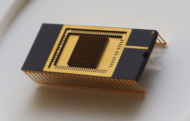
Samsung announced Tuesday that it would roll out the world’s first 3-D vertical NAND flash memory this month, claiming that the technology would end memory scaling problems.
While the firm declined to comment, industry watchers predicted that Samsung would be applying its 3-D flash memory to its devices by as early as the end of this year.
“Samsung will continue to keep the current 2-D flash memory production lines in operation for a while, but will eventually replace them with those for the 3-D technology,” said Choi Jeong-hyuk, a senior vice president of Samsung’s memory business department.
He added that, “the 3-D flash technology has been developed after years of relentless efforts to overcome the limits of the existing NAND flash technology, and is expected to solidify Samsung’s market leadership.”
 |
Samsung Electronics unveils the industry’s first 128-gigabit 3-D vertical NAND flash memory on Tuesday. (Yonhap News) |
NAND flash memory is a storage technology that is an essential part of laptops and tablets. However, it has been known to suffer from reliability issues as its capacity increases.
Choi likened the 3-D V-NAND to a skyscraper as the cells are stacked on top of each other in up to 24 layers, a technology developed by the tech firm over about 10 years to overcome the scaling limits of conventional NAND memory in which cells are aligned on a grid.
The new memory performs twice as fast as conventional 10 nanometer-class NAND flash memory, according to Samsung.
Previously, as the manufacturing process technology proceeded to the 10nm-class, meaning a process technology node between 10 and 20 nanometers, and beyond, the 2-D lithography technology reached its scaling limit due to cell-to-cell interference, hampering reliability of NAND flash products.
“This is inevitably the direction the high-end chip makers will have to go because there is a limit to upscaling technology for the existing 2-D chips, which would be at best 15 nanometer-class,” said one industry expert close to the matter.
Samsung’s new V-NAND solves these technical challenges, according to the firm, by revamping its charge trap flash architecture, which was first developed in 2006.
The new technology also involves much capital investment, which is why many chipmakers around the world are having trouble switching to 3-D.
The new 3-D V-NAND will be first commercialized for data centers and servers, and then likely used for a wide range of consumer electronics and enterprise applications including embedded NAND storage and solid state drives.
Choi said Samsung would be able to develop a terabit SSD within five years.
The Seoul-based tech firm’s decision to mass produce the 128-gigabite 3-D flash came a year earlier than market predictions and the firm will likely benefit from its first mover advantage since other competitors such as Intel and SanDisk are reportedly planning larger capacity NAND for the coming years before switching to 3-D NAND.
By Kim Young-won (
wone0102@heraldcorp.com)


![[Today’s K-pop] Blackpink’s Jennie, Lisa invited to Coachella as solo acts](http://res.heraldm.com/phpwas/restmb_idxmake.php?idx=644&simg=/content/image/2024/11/21/20241121050099_0.jpg)


