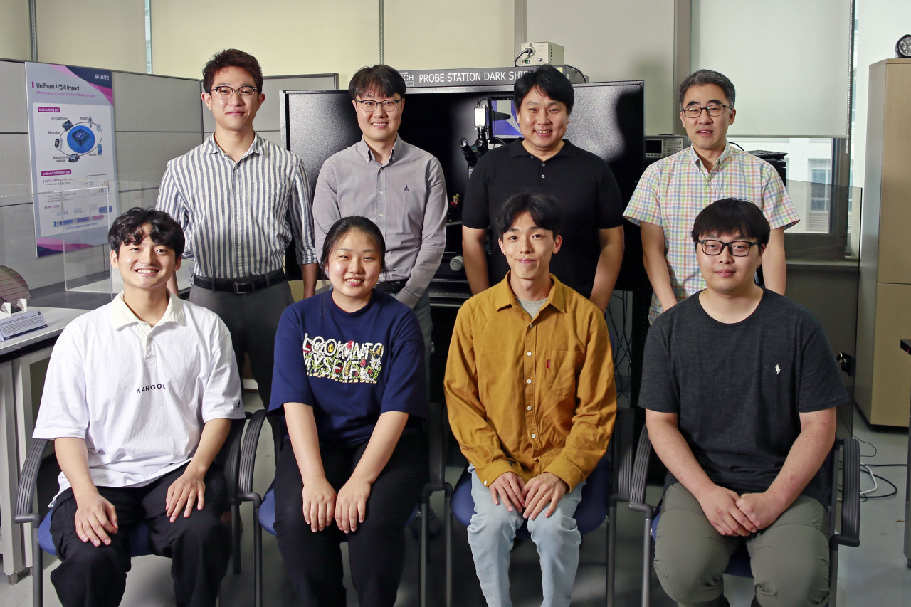
A research team led by Kim Kyung-rok at Ulsan National Institute of Science and Technology successfully implemented the world’s first ternary semiconductor design on a large wafer, which will help development of low-power and high-computing microchips in the future, according to Samsung Electronics on Wednesday.
 |
(Samsung Electronics) |
The ternary semiconductor architecture is expected to contribute to developing high-computing chips that are essential for artificial intelligence, autonomous driving, the internet of things and robotics by enabling reducing the size of chips while improving power efficiency.
Compared to the current binary semiconductors, the new ternary-based chips will shorten data processing time and reduce power consumption.
“The latest research shows that there is a possibility of commercializing ternary semiconductors on the current binary-method chipmaking process technologies, which can lead a change in the paradigm of the semiconductors industry,” Kim said.
Kim’s research theme was selected as one of the future projects funded by Samsung in 2017.
The professor’s team used Samsung’s foundry line for the research.
By Song Su-hyun (
song@heraldcorp.com)


![[Today’s K-pop] Blackpink’s Jennie, Lisa invited to Coachella as solo acts](http://res.heraldm.com/phpwas/restmb_idxmake.php?idx=644&simg=/content/image/2024/11/21/20241121050099_0.jpg)


