 |
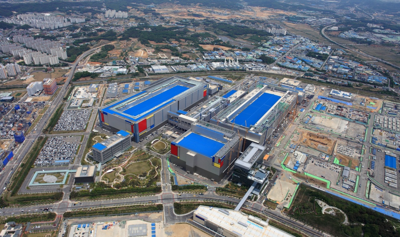
Samsung Electronics’ Pyeongtaek campus (Samsung Electronics) |
Samsung Electronics is preparing to construct another cutting-edge foundry manufacturing line in South Korea, taking one step closer to achieving its goal of becoming the No. 1 system-on-chip business by 2030.
The tech giant on Thursday announced it will break ground for the second extreme ultraviolet foundry line in Pyeongtaek, Gyeonggi Province, this month, with a schedule to start operating the new line in the second half of next year.
Samsung is expected to pour around 10 trillion won ($8.1 billion) for the Pyeongtaek EUV line, according to industry sources.
It is part of Samsung’s 133 trillion won investment plan by 2030.
The company completed the first EVU line, dubbed V1, in Hwaseong in the same province in February, and has been churning out chipsets used for mobile devices, high-performance computing and artificial intelligence on behalf of global customers like Intel, Qualcomm and Baidu.
When President Moon Jae-in visited the construction site for the V1 line last year to announce the government’s vision for the system-on-chip industry, Samsung Electronics Vice Chairman Lee Jae-yong had revealed the chipmaker’s plan to build another EUV line in Pyeongtaek.
While the Hwaseong V1 line is currently dedicated to manufacturing customized chips on 7-nanometer and 6-nm processes, the new Pyeongtaek line will be used for 5-nm process and below.
“The company will expand the volume of chips manufactured on sub-5-nm process in order to respond to the growing demand for EUV-based chips,” said Junng Eun-seung, president of Samsung’s foundry business.
It is too early to estimate the volume expansion, but with full operations of the current V1 line, Samsung aims to boost EUV-based products by three times this year.
The company also said it will continue hiring more engineers dedicated to the foundry business.
Samsung is aggressively increasing investments in the foundry business in a bid to catch up with Taiwan’s TSMC.
The announcement followed TSMC’s decision to construct a foundry factory in the United States. The Taiwanese company will be establishing a 5-nm process-based line in Arizona.
Whether Samsung will expand its manufacturing facility in Austin in order to keep the rival under check remains to be seen.
With the addition of the Pyeongtaek fab, Samsung will have a total of seven foundry production lines located in South Korea and the US, comprised of six 12-inch wafer lines and one 8-inch line.
Regarding the possibility of increasing the Austin facility, Samsung declined to comment.
According to TrendForce, Samsung’s share in the foundry market stood at 15.9 percent in the first quarter, due to declining demand triggered by the COVID-19 outbreak.
TSMC maintained the top spot with a 54.1 percent share during the same period.
By Song Su-hyun (
song@heraldcorp.com)


![[Herald Interview] 'Trump will use tariffs as first line of defense for American manufacturing'](http://res.heraldm.com/phpwas/restmb_idxmake.php?idx=644&simg=/content/image/2024/11/26/20241126050017_0.jpg)
![[Exclusive] Hyundai Mobis eyes closer ties with BYD](http://res.heraldm.com/phpwas/restmb_idxmake.php?idx=644&simg=/content/image/2024/11/25/20241125050044_0.jpg)
