 |
ASML CEO Peter Wennink (right) greets Samsung Electronics Vice Chairman Lee Jae-yong (left) at the Dutch chip equipment giant’s headquarters in Eindhoven, the Netherlands, on Tuesday. (Samsung Electronics) |
Samsung Electronics top executives on Tuesday held talks with representatives of chip photolithography equipment maker ASML, including its Chief Executive Officer Peter Wennink, the South Korean tech giant said Wednesday.
Representatives of Samsung, including Lee Jae-yong, vice chairman and de facto leader; and Kyung Kye-hyun, co-chief executive officer in charge of Samsung’s semiconductor business, visited the headquarters of ASML in Eindhoven, the Netherlands.
Samsung said in a statement that the meeting was held to discuss ways to handle supply issues of ASML’s extreme ultraviolet photolithography solutions, which are considered key to the world‘s most-advanced semiconductor chip manufacturing process. ASML is the sole provider of EUV solutions in the world.
Samsung, a minority shareholder of ASML, did not elaborate further on their discussions.
Tuesday’s meeting came 20 months after Lee and Wennink last met at the ASML headquarters in October 2020.
 |
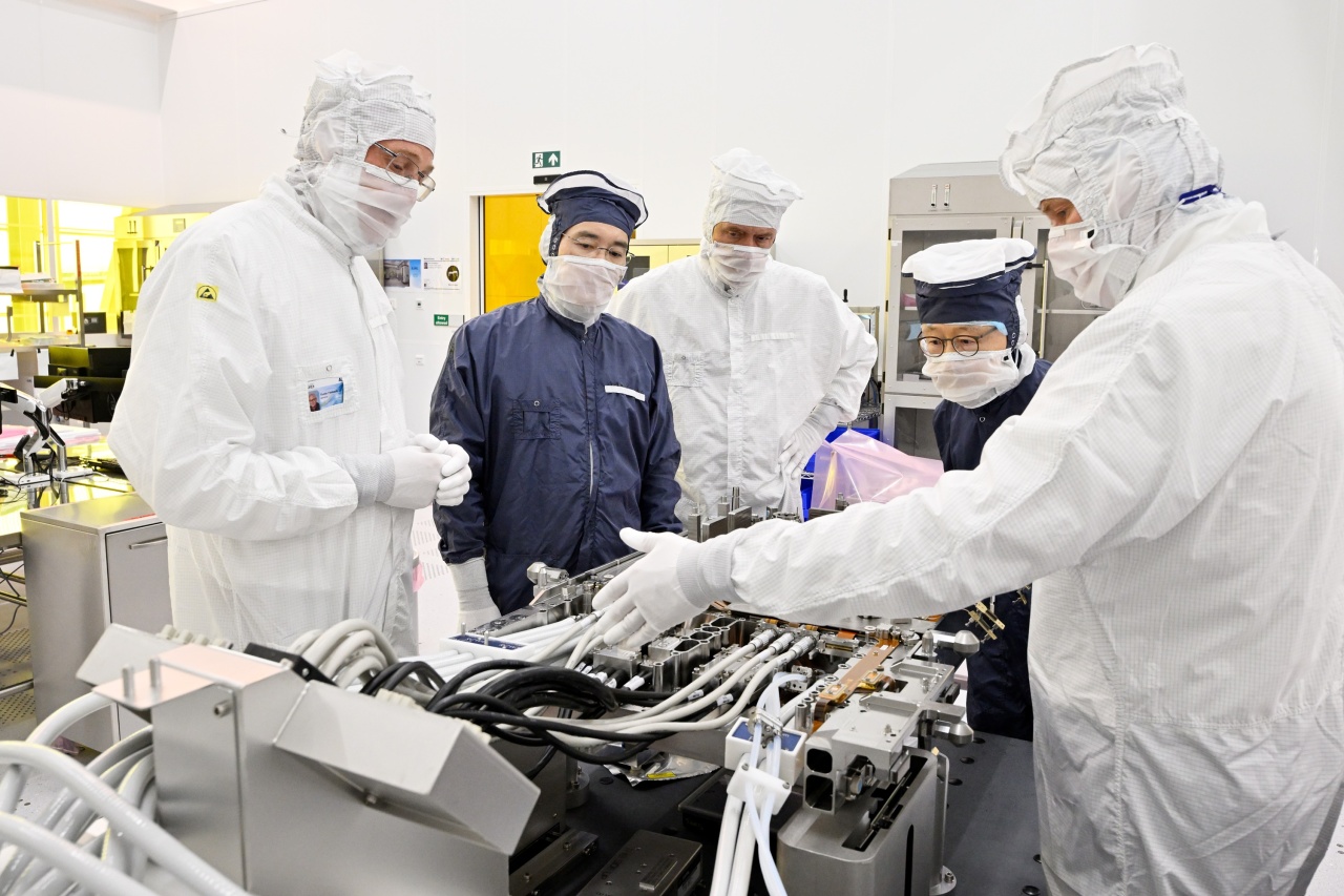
Representatives of Samsung Electronics and ASML, including Samsung Vice Chairman Lee Jae-yong (second from left), check ASML's EUV machine at ASML headquarters in Eindhoven, the Netherlands, on Tuesday. (Samsung Electronics) |
This reflects the world‘s race for high-end semiconductor chips amid chip supply shortage. It also highlights the need to secure the rare equipment, using extremely short wavelengths to print tiny circuit patterns onto wafer-thin materials.
Samsung first adopted the EUV technology in its 7-nanometer process in its contract-based chip manufacturing in 2017. The company also began mass producing 10-nanometer DRAMs in 2020 through EUV process. Its crosstown rival SK hynix moved in tandem, introducing EUV process to its DRAM manufacturing in 2021.
While ASML’s EUV machines have primarily been sold to Korea and Taiwan, home to the world‘s largest foundry TSMC, more chip manufacturers are looking to secure the machines. Intel earlier this year unveiled plans to adopt a 2-nanometer process using ASML’s EUV equipment starting in 2024.
Samsung made a strategic investment in ASML with chip giants Intel and TSMC in 2012. Fewer than 50 EUVs have been manufactured each year.
Lee flew to Belgium to visit Interuniversity Microelectronics Center Wednesday and is scheduled to return home Saturday.
(
consnow@heraldcorp.com)


![[Exclusive] Hyundai Mobis eyes closer ties with BYD](http://res.heraldm.com/phpwas/restmb_idxmake.php?idx=644&simg=/content/image/2024/11/25/20241125050044_0.jpg)
![[Herald Interview] 'Trump will use tariffs as first line of defense for American manufacturing'](http://res.heraldm.com/phpwas/restmb_idxmake.php?idx=644&simg=/content/image/2024/11/26/20241126050017_0.jpg)
![[Herald Review] 'Gangnam B-Side' combines social realism with masterful suspense, performance](http://res.heraldm.com/phpwas/restmb_idxmake.php?idx=644&simg=/content/image/2024/11/25/20241125050072_0.jpg)