Korean researcher makes Nature magazine with nanotech breakthrough
Korean scientists have developed technology that can control the way a solid material cracks for the first time in a breakthrough that could have applications in a range of fields from semiconductors to medicine.
The research was featured on the cover of Wednesday’s issue of Nature. It is the first time a Korean study has been on the cover of the world’s most authoritative scientific journal.
Nam Koo-hyun of Ewha Womans University, who led the research, said his discovery may pave the way for the development of a cheaper and quicker way to produce nano-channels.
 |
Nam Koo-hyun |
His team is the first to discover a technique to control cracking and make use of it, he said.
“The formation of cracks is traditionally considered an unpleasant phenomenon because we thought it is impossible to control,” Nam told The Korea Herald.
Nam’s team used silicon wafers, thin slices of semiconductor material, in their experiment.
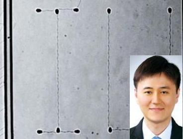
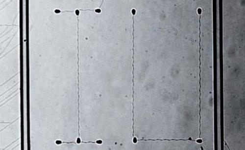
They created micro-scaled cuts in a thin brittle film deposited on the silicon in order to control the starting point of cracking, and put a “crack-stop-structure” to terminate the cracking.
 |
Nam’s team created 10-nanometer-sized channels, which read I.U., the name of a Korean pop singer, by controlling cracking patterns. |
“By doing this we can place the starting point of cracking very precisely, and even control the direction of the cracks and bend them around corners,” Nam told The Korea Herald.
The nano-channels that are small enough to allow ions or molecules of a certain size to pass through are highly in demand in chemistry and molecular biology, such as DNA analysis.
But until now it has been difficult to make individual artificial channels of such a small size with current fabrication technique.
The team, however, suggests they can produce nano-channels more easily by using their cracking-control method. They had already made artificial channels that are merely 10 nanometers in size during their experiment.
“We would finally be able to reach to the artificial atomic-scale patterning if wild crack is well controlled. This is a good start for such a big goal,” Nam said.
The researcher, however, admitted that there are still limitations in their technique as it was proven in just several materials.
“We cannot say at the moment that crack control can be achieved with any materials,” he said. “But at the same time we can say that there are many other materials to find a lot of interesting crack control.”
The Ministry of Education, Science and Technology, which funded the project, said the discovery will open a new chapter in Korean science.
By Oh Kyu-wook (
596story@heraldcorp.com)
용접공 출신 '남박사' 세계굴지 과학잡지에
이화여대 초기우주과학기술연구소 남구현(33) 특임교수가 이끈 연구팀이 세계 최고의 과학저널인 영국 네이처지(誌) 10일자에 '균열 제어를 통한 형상 구현(Patterning by controlled cracking)'이란 논문을 발표했다.
반도체 재료인 실리콘 웨이퍼 표면에 인위적으로 균열(crack)을 일으켜 현재 기술로는 구현하기 힘든 나노m 크기의 구조들을 만드는 데 성공했다는 내용이다.
남박사는 90년대 말 외환 위기로 집안이 어려워져 대학 진학을 포기하고 인천 남동공단의 레미콘 공장에서 용접과 산소 절단을 했던 아픈 사연이 있는 것으로 알려졌다.
그러다 2005년 미국 유학을 떠난 후 5년 만에 기계공항박사를 따냈다.
남 교수의 이번 논문은 박사가 된 뒤 첫 논문이다.
네이처지는 전세계 과학자들이 평생 논문 한 편을 실을 수 있을까 말까 할 정도로 논문 심사가 까다로운 것으로 알려져 있다.


