 |
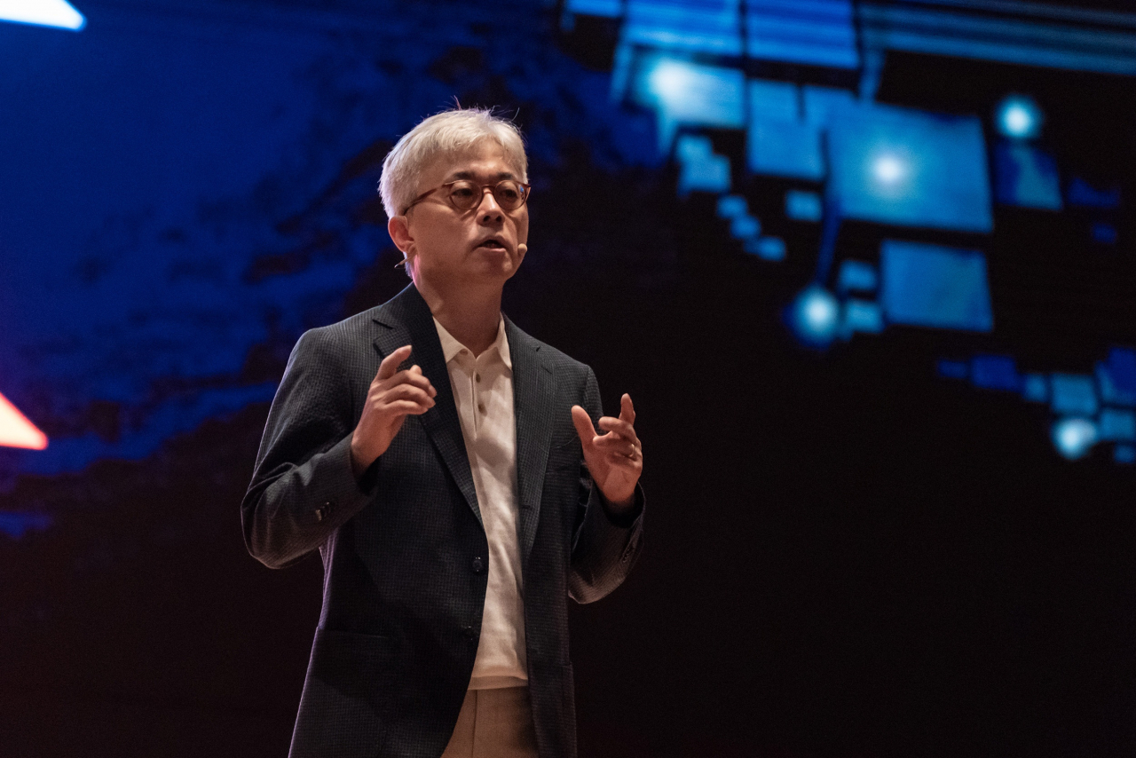
Samsung Electronics President Choi Si-young in charge of the foundry business delivers his keynote speech at the Samsung Foundry Forum 2024 held in Coex, Seoul on Tuesday. (Samsung Electronics) |
Samsung Electronics announced Tuesday it has bagged the first order for its new turnkey semiconductor solutions using the cutting-edge 2-nanometer foundry process from a leading artificial intelligence company in Japan.
Holding the Samsung Foundry Forum and Samsung Advanced Foundry Ecosystem Forum in Seoul, the chip giant also unveiled its foundry strategy for its advanced Gate-All Around transistor architecture to support the local logic chip industry, as well as the latest AI solutions.
Having mass-produced the industry’s first 3 nm process node applying the GAA technology, Samsung said it won an order for the 2 nm process for Preferred Networks in Japan, with further upgrades in performance and power efficiency.
Samsung also applied advanced 2.5D packaging technology Interposer-Cube S for the turnkey chip solution, the company said.
"This order is pivotal as it validates Samsung's 2 nm GAA process technology and Advanced Package technology as an ideal solution for next-generation AI accelerators," said Song Tae-joong, corporate vice president and head of foundry business development at Samsung Electronics.
"We are committed to closely collaborating with our customers ensuring that the high performance and low power characteristics of our products are fully realized," he added.
The 2.5D Advanced Package I-Cube S technology included in the turnkey solutions is a heterogeneous integration package technology, with multiple chips in one package to enhance interconnection speed and reduce package size. The heterogeneous integration packaging technology integrates different types of chips, such as memory, logic and sensors, in a single package.
The use of the silicon interposer is crucial in achieving ultrafine redistribution layer and stabilizing power integrity for optimal semiconductor performance, Samsung said. Gaonchips, a specialized system semiconductor development company, designed the chip.
According to Samsung, the cooperation with Preferred Networks marks the first achievement for a Japanese company in the field of large heterogeneous integrated package technologies. Samsung said it plans to accelerate its leading global advanced package market offensive.
Preferred Networks, headquartered in Tokyo, develops advanced software and hardware technologies by vertically integrating the AI value chain from chips to supercomputers and generative AI foundation models.
Junichiro Makino, vice president and chief technology officer of computing architecture at Preferred Networks, expressed excitement over the collaboration and underscored how Samsung’s solution will “significantly” support his company’s efforts to build highly energy-efficient, high-performance computing hardware.
The company aims to develop powerful AI accelerators that meet the growing demand for computing power driven by generative AI, by leveraging Samsung's foundry and packaging products.
At the forum, Samsung also unveiled the specification of its upcoming High Bandwidth Memory 4 chip, saying it will be "significantly" enhanced compared to the HBM3.
"We will be expanding the processing capacity to 48 gigabytes for HBM4. We plan to start the production of the new product next year," Choi Jang-seok, executive vice president in charge of memory business at Samsung Electronics said.
The company vowed to actively support design solution partners for Korean fabless firms to quickly expand their presence in the high-performance computing and AI sectors.
"Samsung will continue to provide the most needed AI solutions for the customers with specialty solutions such as the BCD solution for AI energy efficiency and high precision sensors enhancing accuracy for edge devices," Samsung Electronics President Choi Si-young in charge of the foundry business said.
Samsung currently supports local customers to apply the latest manufacturing technologies, and the Multi Project Wafer service for the companies to produce prototypes.
The chip giant said companies had used the MPW service 32 times, up 10 percent on-year, and predicted the number to increase to 35 in 2025.
At the forum, 35 partner firms including Telechips, an automotive chip firm, Abov Semiconductors, a designer and manufacturer of microcontrollers, and AI fabless startup Rebellion set up booths to present their solutions for Samsung's foundry clients.
Last month, Samsung held the foundry forum under the theme of "Empowering the AI Revolution" in Silicon Valley. The company plans to hold the event again in Japan and in Europe in the second half of this year.


![[Herald Interview] How Gopizza got big in India](http://res.heraldm.com/phpwas/restmb_idxmake.php?idx=644&simg=/content/image/2024/11/20/20241120050057_0.jpg)