 |
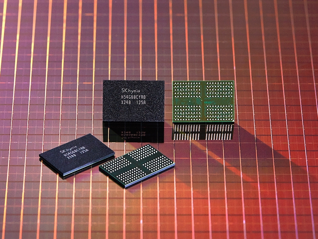
This photo provided by SK hynix Inc. on Monday, shows the company's 1anm DRAM using extreme ultraviolet lithography technology. (SK hynix Inc.) |
SK hynix Inc., the world's second-largest memory chip producer, said Monday it has started the mass production of DRAM with the latest 10-nanometer (nm) process technology.
SK hynix said its 8 Gigabit Lower Power Double Date Rate 4 (LPDDR4) mobile DRAM is built on the 1anm node, using extreme ultraviolet (EUV) lithography technology.
The 1a is the fourth generation of the 10nm DRAM process solution following the 1x, 1y and 1z.
The South Korean chipmaker said it plans to supply the latest mobile DRAM products to smartphone makers from the second half of 2021.
This was the first time that SK hynix used the EUV equipment for mass production following its partial adoption for its 1ynm DRAM products.
SK hynix plans to use the EUV technology for all of its 1anm DRAM production, saying that it has secured the stability of the process.
The company expects the latest node to enhance its productivity. SK hynix said it estimates the 1anm technology to give a 25 percent increase in the number of DRAM chips produced from the size of a wafer compared with the previous 1znm node.
The latest DRAM product stably supports 4266 megabits per second (Mbps), the fastest transfer rate in a standard LPDDR4 mobile DRAM speciation, and has reduced power consumption by 20 percent, according to the company.
SK hynix said it will also apply its 1anm node to its DDR5 products, the world's first next-generation DRAM launched in October 2020, from early 2022. (Yonhap)


