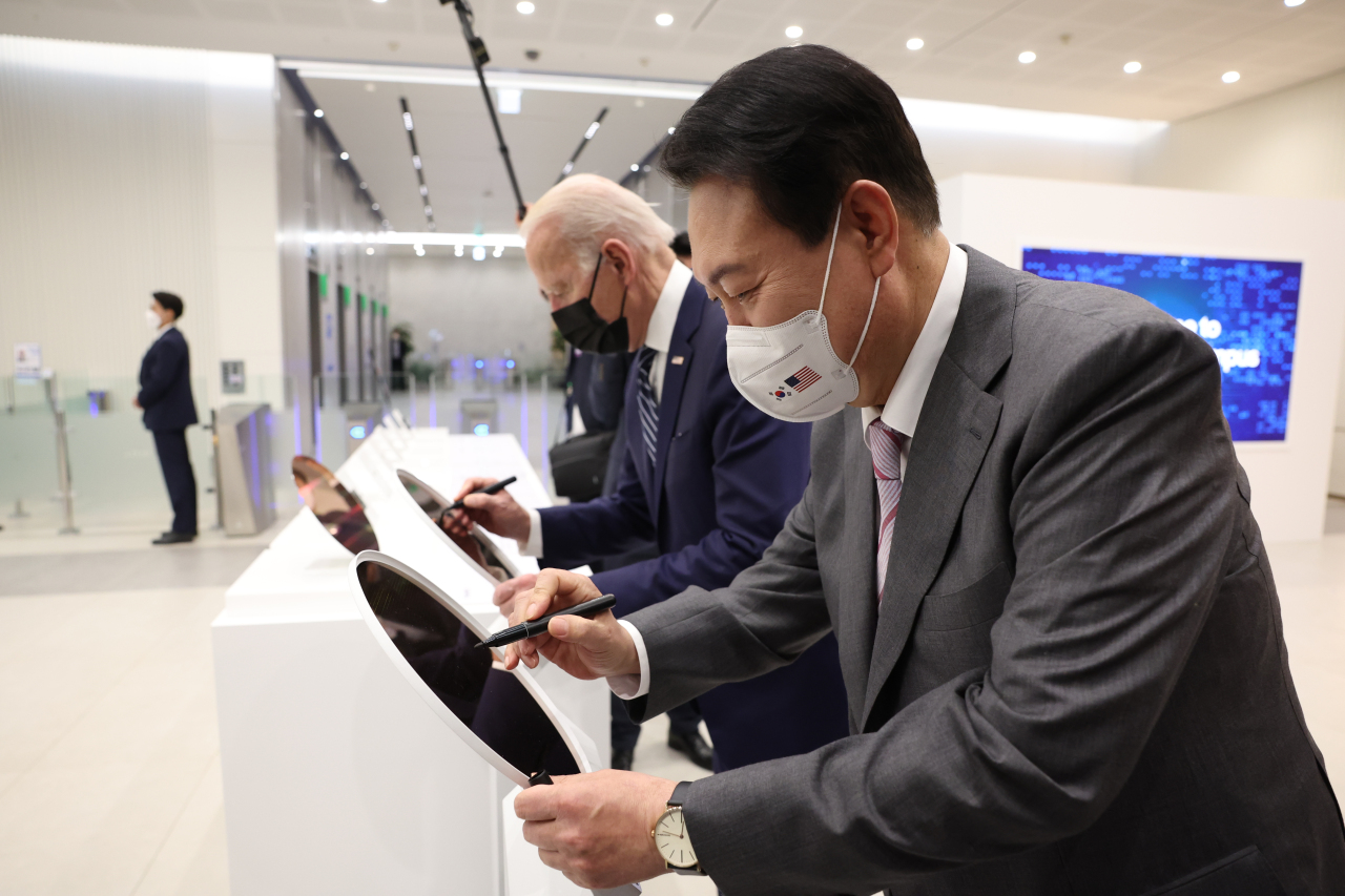
One of the key moments of last week’s summit talks between South Korean President Yoon Suk-yeol and US President Joe Biden was the two signing a semiconductor wafer, not a visitors’ book, during their visit to Samsung Electronics’ chip manufacturing complex in Pyeongtaek, Gyeonggi Province, Friday.
It was the first time that the wafer, produced by Samsung’s new 3 nanometer technology, was unveiled to the public. The Korean tech giant plans to start mass production of the new chips in the coming weeks, an industry first globally.
The 3nm technology boasts greater transistor density than the current 5nm technology, which means higher speed and lower power consumption of advanced chips for artificial intelligence, big data and autonomous cars.
The new technology is a secret weapon for Samsung, the world’s largest memory chip maker, to take on Taiwan’s TSMC, the dominant leader in the lucrative foundry market.
According to industry tracker TrendForce, TSMC took up 52.1 percent of the global foundry market in the fourth quarter last year, while Samsung remained a distant No. 2 with an 18.3 percent share.
Samsung, in particular, is expected to become the first chip maker to roll out 3nm chips using gate-all-around field-effect transistor technology (GAAFET), which has increased the overall efficiency of the current fin field-effect transistor technology (FinFET).
GAAFET reduces power consumption of chips by almost half while improving performance by up to 35 percent, compared to the FinFET.
TSMC also plans to start mass producing the 3nm chips later this year, but would continue to use the FinFET for stability.
“TSMC is choosing stability by sticking to the FinFET for a while, while Samsung is taking risks amid concerns over a lower yield rate in the earlier stage,” an industry source said on condition of anonymity.
“It may be difficult for Samsung to take shares from TSMC immediately, but it could seek an upper hand at least in the nascent 3nm technology.”
The GAAFET is considered essential for the next-generation foundry microfabrication, which is smaller than 3nm, but chip makers are struggling to elevate the yield rate of the highly sophisticated manufacturing technology.
Samsung was no exception. But sources say its yield rate that used to remain at 20 to 30 percent has been greatly improved more recently as the company is bracing for its mass production.
“We have reduced the ramp-up period by enhancing inspection throughout the development process,” said Kang Moon-soo, vice president of Samsung’s foundry business division, during a first-quarter conference call last month.
He also dismissed concerns over profitability, citing robust market demand and strong client partnerships.
When it comes to securing clients and suppliers, many of them based in the US, Biden’s recent visit is likely to offer a big boost, sources say.
Given that Qualcomm CEO Cristiano Amon accompanied the high-profile visit, Samsung’s existing ties with the US chip giant are expected to be further bolstered.
US equipment makers such as Applied Materials and Lam Research that participated in the Korea-US business roundtable meeting held Saturday on the sidelines of the summit talks are also considered key partners for Samsung’s 3nm chips.
Samsung’s chip plant was the first destination of Biden’s three-day visit over the weekend. He was the first US president to visit the 289,000-square-meter site, one of the world’s largest chip manufacturing facilities.
Samsung is also speeding up preparations to start construction work of its new $17 billion foundry plant in Taylor, Texas. The groundbreaking ceremony is set to be held within the first half of this year, with business and political leaders invited to celebrate.
By Lee Ji-yoon (
jylee@heraldcorp.com)


![[Today’s K-pop] Blackpink’s Jennie, Lisa invited to Coachella as solo acts](http://res.heraldm.com/phpwas/restmb_idxmake.php?idx=644&simg=/content/image/2024/11/21/20241121050099_0.jpg)


