 |
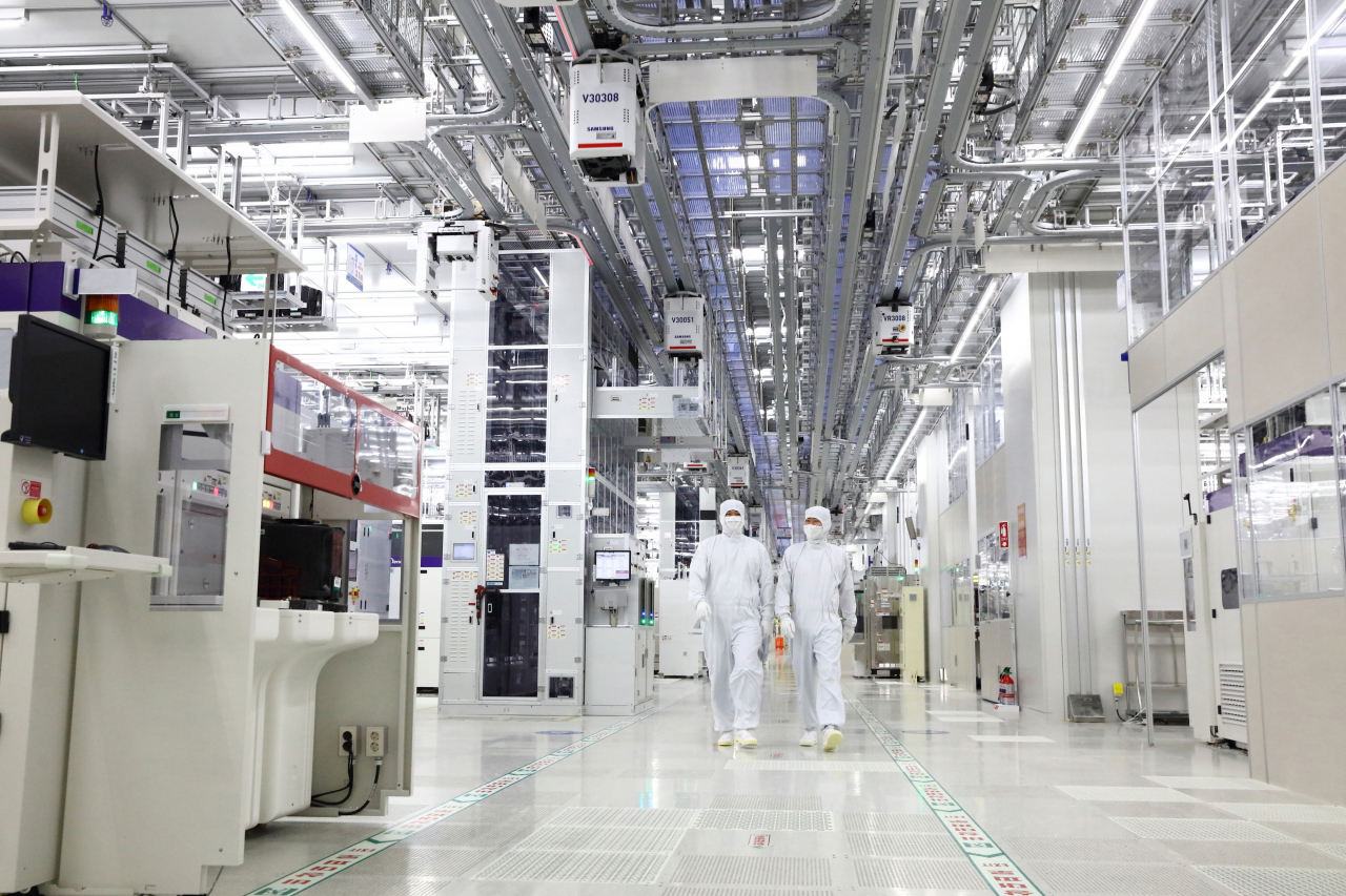
An interior view of Samsung's Pyeongtaek chip plant (Samsung Electronics) |
PYEONGTAEK, Gyeonggi Province -- South Korean tech giant Samsung Electronics is ready to meet the needs of the world's most ambitious chip designers technology-wise in the world's largest single chip fabrication plant.
The multi-story factory, which went operational in July, used enough steel bars to build 29 Eiffel Towers to complete the construction on a plot of land about 25 times the size of a soccer field.
The gargantuan facility, dubbed P3, is the first chip fab to have introduced the cutting-edge extreme ultraviolet photolithography process, among three fabs within Pyeongtaek, Gyeonggi Province, a port city over 60 kilometers south of Seoul.
Opened two months after US President Joe Biden went on a tour there in May -- when the construction was underway -- the fab embraces Samsung's stringent cleanroom standard, automated overhead transport system for chip wafers and various semiconductor equipments.
At the same time, the fab signals Samsung's bid to solidify its position in the global chip industry, with the most advanced semiconductor nodes crucial for more efficient performance and faster data transfer than legacy chips.
The new plant will be capable of manufacturing the DRAM products of the industry's most advanced 14-nanometer process and offer foundry sevices for chip designer clients with 5nm nodes or more advanced ones.
Samsung was the first chipmaker in the world to have started mass producing the 3nm node chips with gate-all-around transistor architecture in July in Hwaseong, another city in Gyeonggi Province, two months ahead of its Taiwan-based foundry service rival TSMC. The Hwaseong location has also come up with the most-advanced 14nm DRAM products labeled as DDR5 or LPDDR5X starting in 2021, using EUV lithography process.
 |
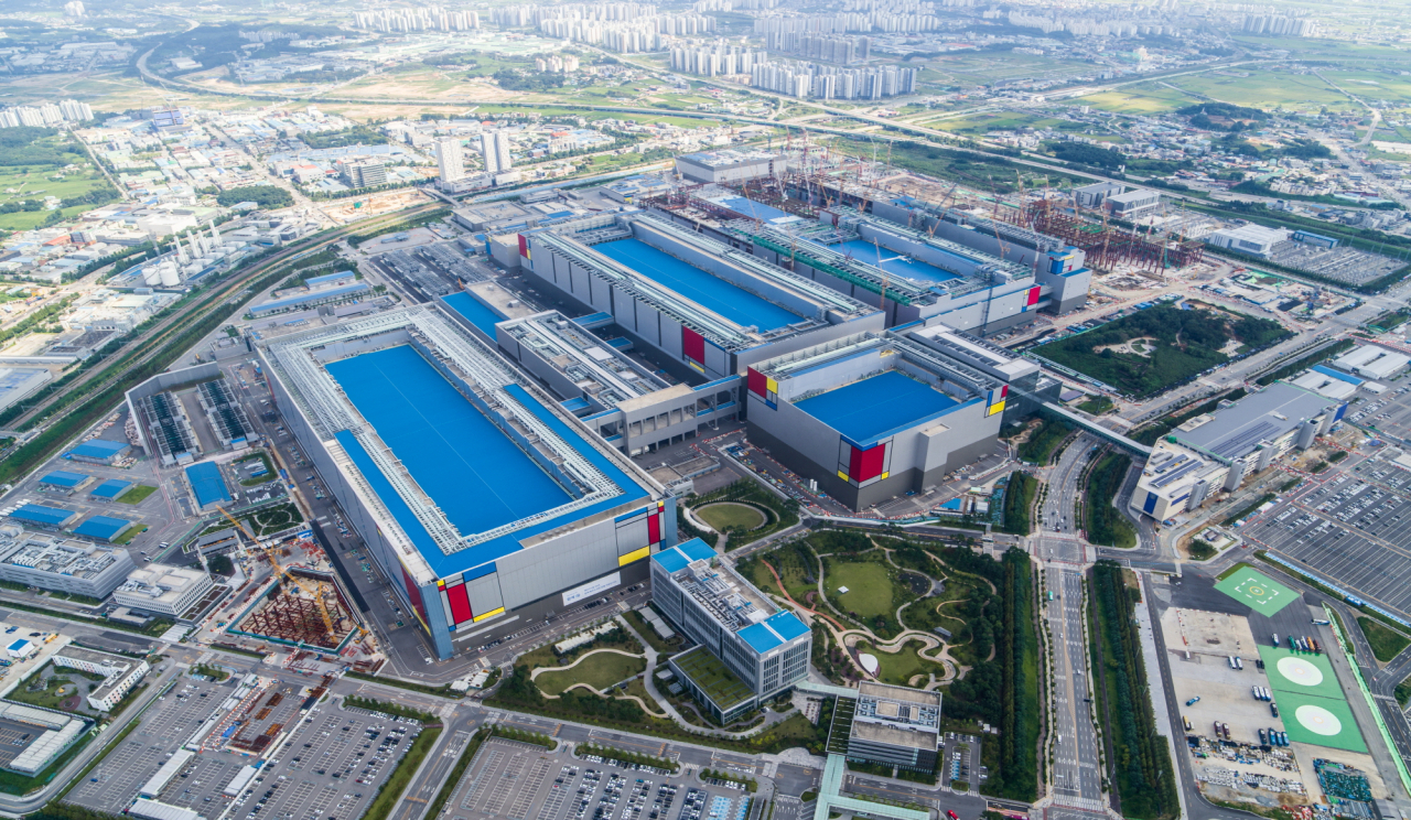
A bird's eye view of Samsung's Pyeongtaek chip plant (Samsung Electronics) |
Samsung's 3nm ambition is not about blazing the trail, but is rather about stabilizing the performance and price of chip products with the next-generation 4nm or 5nm nodes, by expanding the manufacturing capacity .
"By the end of next year, Samsung's foundry services would no longer be what it used to be," Kyung Kye-hyun, co-Chief Executive Officer of Samsung Electronics overseeing semiconductor business, told reporters in a briefing at the Pyeongtaek location.
"Our clients are paying attention to our second generation of 3nm node chips."
But this is only halfway through in Samsung's ambition to transform Pyeongtaek into the world's hottest chip hub, seven years in the making.
Samsung's Pyeongtaek location spans across nearly 2.89 square kilometers, as wide as the total space of chip manufacturing sites in Hwaseong and its neighboring Giheung, combined.
In addition to P1, P2 and P3, the Pyeongtaek site is expecting three more fabrication plants. Samsung has yet to disclose the blueprint for the P4 construction.
At least 1.3 million jobs is to be created by Samsung in the region by 2030 for six fabs, as it currently hires 10,000 Samsung employees and 60,000 workers from Samsung' partner companies.
Samsung's ambition, the other way around, translates into a desperate bid to weather the chip down cycle and trounce Chinese and US players in cutthroat chip competition amid supply chain uncertainties.
The memory chip industry is witnessing heated competitions by Chinese firms, especially in NAND Flash products. Samsung has been confident in having the upper edge in DRAM technology and keeping pricing competitive, but Apple's approval of Chinese state-backed chipmaker YMTC as the new NAND Flash memory supplier for its latest flagship iPhone 14 signals Chinese memory firms' greater clout in the industry long dominated by Samsung and crosstown rival SK hynix.
 |
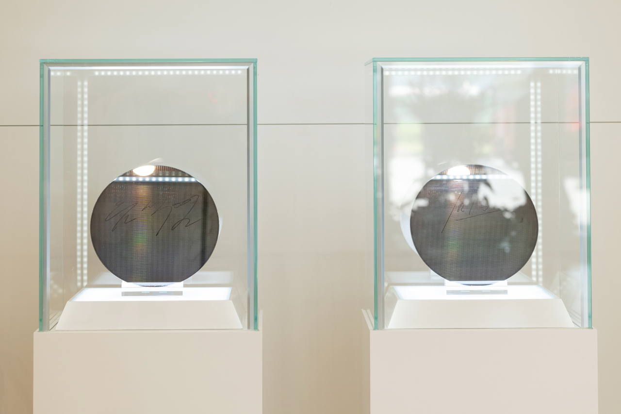
Semiconductor wafers signed by President Yoon Suk-yeol and US counterpart Joe Biden are displayed at Samsung's Pyeongtaek chip plant. (Samsung Electronics) |
The key to competitive edge, especially in times of crisis, is Samsung's relentless investment push for a stronger research and development capability, Kyung said.
"The chip down cycle is likely to persist in the second half, and now I don't see a momentum for a rebound in the next year to come," Kyung said.
"But I believe that consistency in investment plan regardless of the prospects of the ups and downs makes more sense in general than investing through ups and downs."


