 |
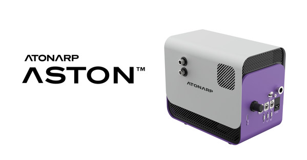
TOKYO, July 15, 2021 /PRNewswire/ -- Atonarp, a leading manufacturer of molecular sensing and diagnostics products for the semiconductor, healthcare, and pharma industries, today announced Aston, an innovative in-situ semiconductor metrology platform with an integrated plasma ionization source.

Aston is a major evolution in metrology for semiconductor production processes, enabling in-situ molecular process control and allowing existing fabs to run more efficiently, driving higher output. Built from the ground up for semiconductor production, Aston is a robust platform that can replace multiple legacy tools and provide unprecedented levels of control across a comprehensive set of applications, including lithography, dielectric and conductive etch and deposition, chamber clean, chamber matching, and abatement.
"With Aston, we've seen unit process throughput increases exceeding 40% in certain applications – that's a big improvement. Even a 1% improvement in overall fab throughput can add up to tens of millions of dollars a year in production for a typical fab," said Prakash Murthy, CEO, CTO, and founder of Atonarp.
"Retrofitting Aston to an existing production process tool can deliver greater throughput within just six to eight weeks, compared to up to a year when installing new production equipment," said Murthy. "This will materially help manufacturers increase their production levels and help to address the current shortage of semiconductor fab capacity."
Rapid, actionable endpoint detection (EPD) is the most efficient way to run a semiconductor tool and fab. Until now, EPD could not be deployed in many process steps because the required in-situ sensor would not survive the harsh process or chamber cleaning chemicals, or would alternatively suffer clogging from condensate deposits. Historically, fabs were forced to use a fixed time in order to ensure that a process was complete. Conversely, Aston optimizes production by detecting exactly when a process has finished, including chamber cleaning, which can reduce the required clean-time by up to 80%.
Aston is resistant to corrosive gases and gaseous contaminant condensates. It is more robust than existing solutions, featuring independent dual ionization sources – a classic electron impact ionization source and a filament-less plasma ionizer – that work reliably in the harsh conditions encountered in semiconductor production. This enables Aston to be used in-situ, in demanding environments where traditional electron ionizers would corrode and fail very rapidly.
Aston offers an interval between service events that is up to 100 times longer compared to legacy mass analyzers. It includes self-cleaning capability that eliminates the build-up resulting from the deposition of condensates present in certain processes.
Since Aston generates its own plasma, it works with or without process plasma present. This provides a clear advantage over optical emission spectroscopy metrology techniques, which require a plasma source to operate, making Aston ideal for ALD and certain metal deposition processes that may use a weak, pulsed, or no plasma for processing.
Aston also delivers improved process consistency by offering quantified, actionable, real-time data, facilitating powerful machine learning via artificial intelligence (AI) for the most demanding process applications. This is in addition to enhanced line and product yields, thanks to high accuracy, sensitivity, and repeatability for statistical analysis of real-time data and process chamber management.
Aston is primarily aimed at use with chemical vapour deposition (CVD) and etching applications, both of which are registering annual growth rates in their usage exceeding 13%. The spectrometer can either be installed within new process chambers during their assembly, or retrofitted into existing chambers already in operation.
Aston can also be used with Psi, an intelligent pressure controller developed by ATI Korea. After undergoing a comprehensive, multi-month technical feasibility evaluation, this combined solution was recently purchased by Samsung for an advanced process control application.
Aston is now available for evaluation and ordering, through either direct purchase or Atonarp's global partner network.
About Atonarp
Atonarp is leading the digital transformation of molecular sensing and diagnostics for life sciences, pharmaceutical, and semiconductor markets. Powered by a unifying software platform and breakthrough innovations in optical and mass spectrometer technology, Atonarp products deliver real-time, actionable, comprehensive molecular profiling data. Led by a world-class team of experts in the development and commercialization of semiconductor, life sciences, and health diagnostic instruments, Atonarp has operations in Japan, the United States, and India. Learn more at https://atonarp.com.
Related Links :
http://www.atonarp.com


